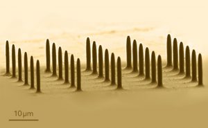
Part 1: Focused Electron Beam Induced 3D Nanoprinting
Part 2: 2-Photon Polymerization
August 9, 2017
Last edited: May 3, 2022
3D printing or its industry-common synonym additive manufacturing is already an indispensable part of many industries. Traditionally used for prototyping, 3D printing currently enables manufacturing of highly complex structures e.g. prosthetics, machine parts, etc., thanks to its layer-by-layer manufacturing mentality. There are many widely used 3D printing technologies out there, that have mostly nothing to do with each other. If you are interested in these technologies, please visit one of the best technical resources I came across online: the Hubs website. If you are also interested in knowing how you can 3D print a model of a city or an army of nanorobots on the surface of a single hair, just keep on reading these post series.
As a nanoscientist and a 3D modeling/printing enthusiast, it was natural for me to dig into the intersection of these areas. The following several posts in this series are an outcome of a research on the limits of resolution of 3D printing – which is currently sub-nanometer. There are already very good scientific reviews about the lab-scale applications so I narrowed the focus down to commercially available printers/printing services offering at least sub micrometer precision. Even then these posts are far from being a complete review but I wanted to share my excitement about what I have encountered.
Part 1: Focused Electron Beam Induced 3D Nanoprinting
Nanoscale Systems (Nanoss) GmbH is a spin-off of the Johann Wolfgang Goethe-University Frankfurt / Germany. They define themselves as “The Medical Sensors Company” and describe their flagship technology nano3DSense as “The First 3D Printer with True Nanometer Precision“. Before going into the technical details of the printing technology they use, please watch this impressive video of the printing process in real time:
The technology that makes nano3DSense‘s high precision printing possible is a technology called (gas-assisted) focused electron beam induced deposition (FEBID). This technology has apparently existed for decades but its use has been limited to research purposes. Nanoscale Systems seems to have commercialized this method (currently) for development of nanoscale mechanical sensors. Printing with FEBID takes place in a scanning electron microscope (SEM), so in high vacuum. According to the company, printing can be achieved on almost any surface. Company’s website refers to a Nature Communications article [1] for technical details of the printing process but I would like to cite from this review article [2] for a very concise description of FEBID: “The basic principle […] is quite simple. Gas molecules (most commonly metal-organic molecules) are adsorbed on a substrate. Under the influence of the e-beam, the precursor molecules are dissociated into volatile and non-volatile components […] (T)he nonvolatile components adhere to the substrate and form a deposit […] Hence, a structure is grown...”
So how nano3DSense prints the sensors is: (1) A special compound in gaseous phase is injected (sprayed) with a very thin needle on an area including the area to be printed. (2) The molecules of the injected compound are adsorbed on the substrate (3) An electron beam is pointed exactly onto the area of interest in a scanning fashion. (4) The interaction of the adsorbed precursor molecules and electrons creates insoluble solid nanoparticles fixed in a carbon matrix. (5) The deposition process continues until the desired 3D structure forms. An important point here is that this technology can only control the size and position of the electron beam with nanometer resolution. The compound is sprayed onto a much larger area.
Company’s website describes the final printed material as “(H)ighly robust nanocomposite material which normally consists of nanogranular metallic clusters, randomly embedded in a carbonaceous matrix“. As far as I could find from literature, the gaseous precursor compound is trimethylmethylcyclopentadienylplatinum(IV) [MeCpPt(Me)3] and the final structure consists of Pt nanoparticles embedded in a carbon structure. It should be an expensive process though: as of August 2017, Sigma-Aldrich lists 2g of MeCpPt(Me)3 for around 800€. Add to this also the requirement of a scanning electron microscope and the qualified staff. But then, going nano costs…
On the other hand, Nanoscale Systems claims their technology might be a strong alternative to more expensive, time-consuming clean room (lithography based) printing methods in some cases. This video presentation is a good comparison of the lithography based printing (top-down) and electron-beam based printing (bottom-up). My tip is to watch this at 2x speed:
I will not go into the details of the current applications of this high-resolution 3D-printing technology. One of the most promising applications is, though manufacturing nanogranular tunneling resistors or NTRs. NTRs can, for one, enable the use of extremely small and sensitive AFM cantilevers. The authors of the above-mentioned Nature Communications article state that “(W)e have shown in this paper the use of NTR sensors for AFM cantilever sensing […] the same sensor and rapid prototyping technology can also be used in cantilever-based bio sensors, 3D MEMS and nano-electro-mechanical systems (NEMS) devices, as well as strain-field sensing on flexible membranes such as those currently used in neural interfaces“.
It is hard to guess how affordable this technology will be in the near future. I think it has a big potential to become a common way of building nanosensors and other extremely small structures, regardless of the costs. A very recent article in Science Advances, for example, reports a solution-based electrochemical electron beam lithography in contrast to the existing gas-assisted processes (the article is not open access, sorry). Once commercialized, nanoclusters of many common materials (gold, copper, nickel) can be printed and erased with nanometer precision on-demand! I will be following advances in electron beam induced printing methods and share any interesting information in future posts. Until then, the resources below should be helpful.
More about focused electron beam induced deposition
[1] https://www.nature.com/articles/ncomms12487 (open access)
[2] http://aip.scitation.org/doi/10.1063/1.2977587 (requires access)
https://en.wikipedia.org/wiki/Electron_beam-induced_deposition
http://avs.scitation.org/doi/abs/10.1116/1.2955728 (requires access)
https://www.beilstein-journals.org/bjnano/articles/3/70 (open access)
Following posts in the series
1-) 2-photon polymerization direct laser writing tool:

Brandenburg Gate made really small! Taken from http://www.nanoscribe.de/en/applications/micro-rapid-prototyping/
2-) Cytosurge’s creative AFM based 3D microprinting

Highly precise micropins. Taken from https://www.cytosurge.com/page/micro3dprinting
Çağrı Üzüm
Disclaimer: This is a personal blog. I write about things that I find exciting and think are worth sharing. The content was not influenced by advertising or sponsorship. There may be other great products from other companies that I am not aware of (actually I would appreciate if you could write to me if you know any).

This work is licensed under a Creative Commons Attribution-NonCommercial 4.0 International License.